Sign In | Join Free | My entremaqueros.com
China Shenzhen Jiaqing Circuit Co., Ltd. logo
Shenzhen Jiaqing Circuit Co., Ltd.
Verified Supplier

1 Years

Home > Multilayer PCB >

4 layer PCB

Shenzhen Jiaqing Circuit Co., Ltd.
Trust Seal
Verified Supplier
Credit Check
Supplier Assessment
Contact Now

4 layer PCB

Model Number : 4L-PCB-1.6mm

Min Trace/Space : 3mil(0.075mm)

Price : negotiate

Finished Thickness : 0.3-16.0mm

Certification : GB/T 19001-2016/IS0 9001:2015

MOQ : 1PCS

Delivery Time : 5-15 Werktage, Eilbestellung möglich

Solder Mask Color : Green, White, Red, Black

Payment Terms : L/C,D/A,D/P,T/T

Layer Count : 4 Layers

Surface Finish : Immersion Gold, OSP, Lead-free HASL

Copper Weight : 0.5OZ-15OZ

Supply Ability : 20000 Quadratmeter / Monat

Material : FR4

Application : Consumer Electronics, Industrial Control

Brand Name : JQPCB

Board Type : Multilayer PCB

Packaging Details : Vakuumverpackung + Antistatikbeutel, Trockenmittel, Temperaturanzeigekarte, Karton

Place of Origin : China

MOQ : 1 Piece

Contact Now

4 Layer PCB4 layer PCB

Design Principle of 4 Layer PCB

The standard 4-layer PCB stackup is usually TOP (Signal) - GND2 (Ground Plane) - PWR3 (Power Plane) - BOTTOM (Signal). Ground and power inner planes provide stable reference potential, greatly reduce signal crosstalk and EMI interference. This stack structure improves signal integrity, ideal for circuits with power supply isolation and high-speed signal transmission. Design tips: Route critical high-speed traces adjacent to ground planes; avoid traces crossing split power/ground areas.

4 layer PCB

PCB Manufacturing Process

  1. Gerber & stackup review: Check design files, DFM audit, confirm layer stack, impedance requirement and special process.
  2. Inner layer fabrication: Copper etching for inner power/ground layers, AOI inspection.
  3. Lamination: Prepreg and copper foil lamination under high temperature and pressure to bond 4 layers together.
  4. Drilling & Desmear: Mechanical drill plated through holes, remove resin smear inside holes.
  5. Copper plating: Electroless copper + electroplating to connect all layers.
  6. Outer layer circuit: Exposure, developing, etching for TOP/BOTTOM traces, AOI test.
  7. Solder mask coating: Apply green/red/black/white solder mask, expose & develop.
  8. Surface finish: Immersion Gold / OSP / Lead-free HASL as requested.
  9. Silkscreen printing: Print component marks, logos and part numbers.
  10. Routing/V-scoring: Depanel boards, electrical test, final inspection & packaging.

Technical Difficulties & Key Process Notes

  1. Lamination control: Strict temperature-pressure curve to prevent layer shift, bow & twist, resin void.
  2. Hole plating quality: Ensure uniform copper deposition in through holes; avoid hole breakage or poor interlayer connection.
  3. Impedance control: If impedance required, copper thickness, prepreg thickness must be precisely controlled during lamination.
  4. Min trace & space: Our minimum trace/space can reach 3mil(0.075mm). Fine lines require precise exposure and etching control.
  5. Solder mask on small pads: Prevent solder mask bridging on dense fine-pitch pads.
  6. DFM suggestion: Avoid oversized split planes; maintain enough clearance between traces and plane gaps.

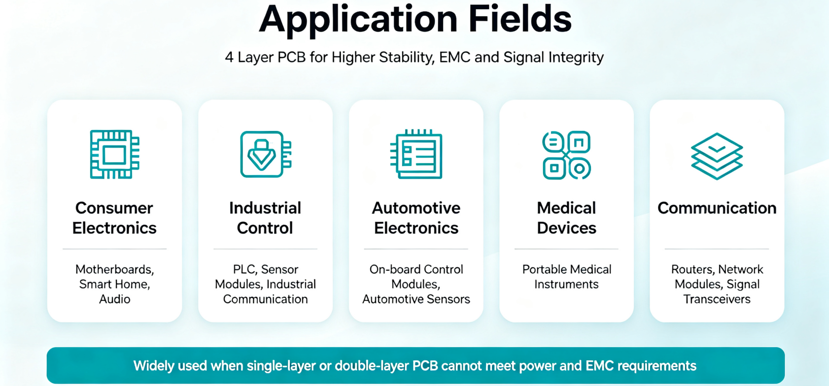
Application Fields4 layer PCB

4 layer PCB is widely used when single/double layer PCB cannot meet power and EMC requirements.

  • Consumer electronics: Motherboards, smart home devices, audio equipment
  • Industrial control: PLC, sensor modules, industrial communication boards
  • Automotive electronics: On-board control modules, automotive sensors
  • Medical devices: Portable medical instruments
  • Communication: Routers, network modules, signal transceivers

JQPCB Advantage4 layer PCB

We support custom 4 layer PCB prototype and mass production, strictly follow IPC-A-600 standard. We provide DFM check before production to reduce design risk. Send your Gerber files for quotation.


 4 layer PCB Manufactures

4 layer PCB Images

Inquiry Cart 0
Send your message to this supplier
 
*From:
*To: Shenzhen Jiaqing Circuit Co., Ltd.
*Subject:
*Message:
Characters Remaining: (0/3000)